
Epitaxial Lift-Off (ELO) is a patented [1] technology approach pioneered at RBU, where the expensive Ge or GaAs substrate wafer is removed from the III-V photo-sensitive layers in such a way that it can be reused.
For this purpose a few nm thick release layer is deposited before the actual III-V cell structure. This sacrificial layer allows for the separation of the device structure from its native semi-conductor wafer by selective wet etching using an aqueous HF solution [2]. The thin, single crystal cell structures obtained by the ELO technology can be mounted on low cost foreign carriers like metal or plastic foil for stability during further processing. The fact that these carriers can be selected on the basis of their material properties rather than crystal growth demands, opens the way for the development of new innovative device structures. Owing to the large selectivity (>106) of the etching process, the expensive semiconductor wafer is not affected and can be reused many times as a production platform of subsequent thin-film cells [3].
At RBU and tf2 the technology can be applied to III-V cells from any supplier of epi-structures if the thin-film structure on the wafer is properly prepared to enable the ELO process step.
The re-use of the wafer implies a drastic reduction of the cell costs. A five times reuse of the wafer would result in an approximate 30% cost reduction of the solar cells, but recent advances of the ELO technique promises a much more frequent reuse which drives cell production cost down by half of its original cell cost.
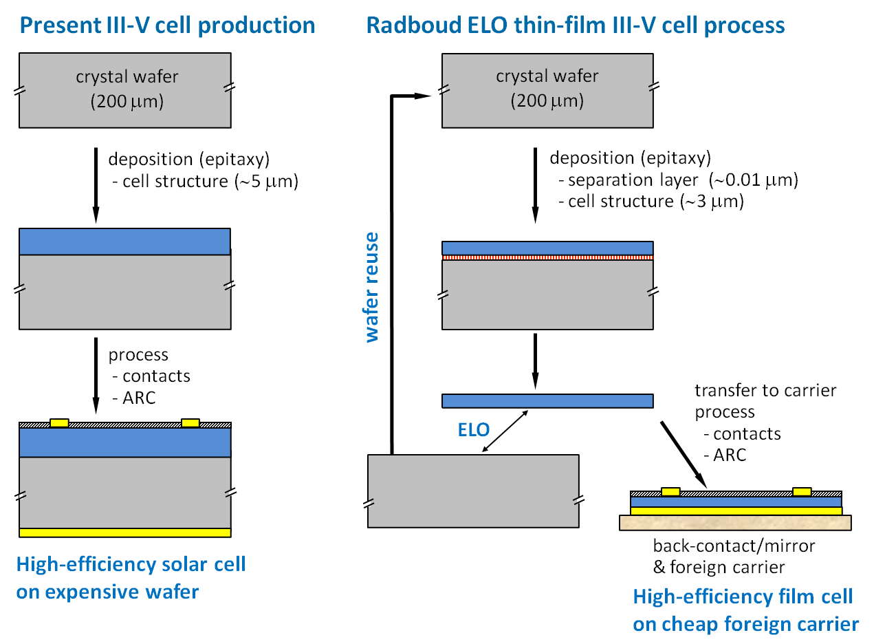
Not-to-scale illustration of the current III-V wafer based cell production compared to the ELO thin-film cell processing. Because of the mirror back-contact also the active cell structure can be reduced to approximately half the thickness required for a wafer based cell structure.
[1] J.J. Schermer, “A method for separating a film and a substrate” patent 01982937.3-2307PCT / NL0100765 1328403/US6974521 (2002).
[2] G.J. Bauhuis, P. Mulder, J.J. Schermer: “Thin-film III-V solar cells using epitaxial lift-off” Chapter 21 in: “High-efficiency solar cells: physics, materials and devices” X. Wang, Z.M. Wang (eds.), Springer Int. Pub., [3] M.A. Green, K. Emery, Y. Hishikawa, W. Warta, E.D. Dunlop, “Solar cell efficiency tables (version 45)”, Prog. Photovolt: Res. Appl. 23, 1 (2015).
[3] G.J. Bauhuis, P. Mulder, E.J. Haverkamp, J.J. Schermer, E. Bongers, G. Oomen, W. Köstler, G. Strobl, “Wafer reuse for repeated growth of III-V solar cells”, Prog. Photovolt: Res. Appl. 18, 155 (2010).