
The fabrication technology of the nanophotonic gratings based on replication by Nanoimprint Lithography (NIL) allows to pattern even subwavelength period gratings over large areas. NIL provides cost efficient mass production possibility for the final product. The main part of the nanolithography costs when employing NIL technique, besides the labour and capital expenses, is the cost of the wafer- masters. Since the master can be replicated up to ~100 times, mass production enabled by NIL can bring the cost of nanostructuring down to few euros for each wafer. Using NIL wafers with a sizes of up to 6” can be patterned in single step. Moreover, given the fact that NIL can be integrated as part of normal process flow to define contact-grids, the cost and scalability of the NIL processes is deemed to be significantly cheaper than standard deposition of dielectric films. Nanostructured moth-eye structures with broadband antireflection characteristics demonstrated by TUT were realized by applying NIL to the AlInP window layer of GaAs-based solar cells [1].
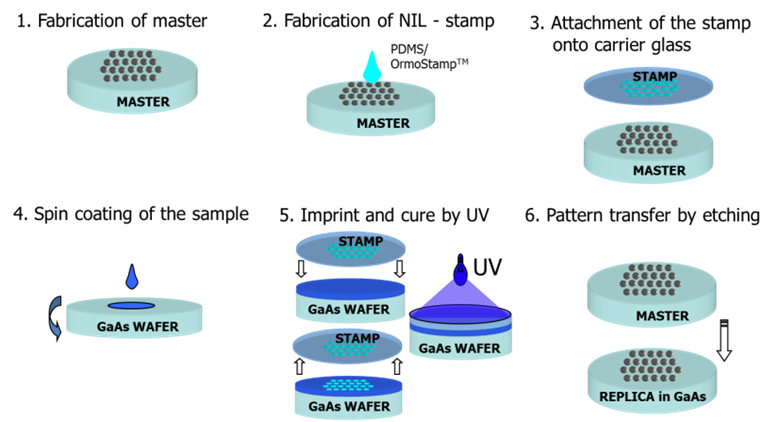
Fabrication process of the nanophotonic gratings by Nanoimprint Lithography
[1] Tommila, J., Polojrvi, V., Aho, A., Tukiainen, A., Viheril, J., Salmi, J., Schramm, A., Kontio, J.M., Turtiainen, A., Niemi, T., Guina, M., Nanostructured broadband antireflection coatings on AlInP fabricated by nanoimprint lithography, Solar Energy Materials and Solar Cells, 94 (10), pp. 1845-1848 (2010).